

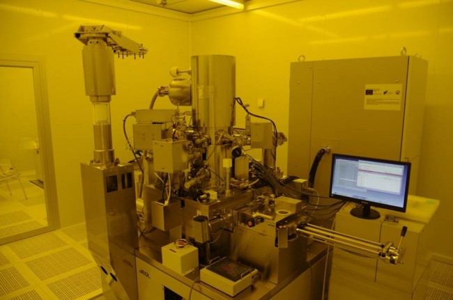
E-beam lithography is the technology created for microelectronics and meets all OVD’s requirements for resolution, flexibility and performance. This technique makes it possible of arbitrary topology creation while extreme resolution of nanometer scale allows utilizing the recent development of digital holography.
The e-beam holograms are capable to control the light field (amplitude and phase of the light) as well as its polarization. Sub-micron structures with specific 3D profiles can produce unique optical effect such as 3D visualization, motion, color selectivity and much more complicated security futures.
That is the reason why we choose the e-beam lithography as our primary holograms’ mastering technology.


